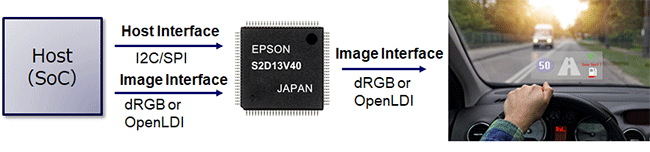
T he S2D13V40 is a warping correction controller IC specific to Head Up Display. It features an internal Surface Correction Engine which fixes visual distortions caused by non-linear display surfaces. It is also able to simultaneously perform other image manipulations such as rotation and scaling.
The S2D13V40 is qualified for automotive design including AEC-Q100/IATF16949 certification and comprehensive safety features. The S2D13V40 can be easily inserted into existing system display architectures with minimal modifications required, making it an ideal solution for both existing and future designs.
|
Part Number |
S2D13V40 |
|---|---|
|
Power Supply |
3.3V(I/O) / 1.8V(Internal) |
|
Input Interface |
OpenLDI/dRGB (Selectable) |
|
Output Interface |
Open LDI / dRGB (Selectable) |
|
Host Interface |
SPI/I2C |
|
Resolution |
Max : ~2880 x 1080 or 2400 x 1400@60fps |
| Host Interface | SPI/I2C |
|
Resolution |
Up to 800x600 (24bit) |
|
Safety Features |
Comprehensive Safety Features |
|
Automotive QA |
AEC-Q100 |
|
Operating Temperature |
-40~+105℃ |
|
Miscellaneous |
Internal PLL |
|
Internal SSCG |
|
| Briefsheet | |
|
Package |
QFP15-100PIN(P-LQFP100-1414-0.50) |
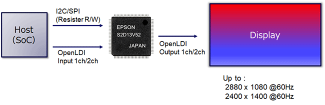
 The S2D13V52 is a Scaler used to upscale/downscale streaming image data from one resolution to another. An internal line buffer and special synchronization logic provide seamless transition from one display resolution to another. A full frame buffer is not required. Customer can develop optional resolution display system with existing Host CPU. S2D13V52 is qualified for automotive design including AEC Q100/IATF16949 compliance and several error detection features. Other features include a double buffered LUT for gamma correction, self-test image pattern generation, input crop, area blanking.
|
Part Number |
S2D13V52 |
|---|---|
|
Power Supply |
3.3V(I/O) / 1.8V(Internal) |
|
Input Interface |
OpenLDI-Rx (1ch/2ch) |
|
Output Interface |
OpenLDI-Tx (1ch/2ch) |
|
Input Resolution |
Max : ~1920 x 1080@60fps |
|
Output Resolution |
Max : ~2880 x 1080 or 2400 x 1400@60fps |
| Host Interface | SPI/I2C |
|
Image Correction |
Gamma Correction |
|
Error Detection |
Input Video Data CRC Check |
|
Automotive QA |
AEC-Q100 Qualifiaction |
|
Miscellaneous |
Internal PLL |
| Package |
H4QFP15-100-pin (14mm x 14mm ,t=1.7mm, 0.5mm pitch) |
| Briefsheet | |
| Status | Under Development |
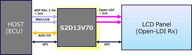
S 2D13V70 is an eDP(rev.1.4a) to Open LDI bridge device which can realize the connectivity between the eDP source to the display panel with the Open LDI interface. It can receive the data rate of 1.62Gbps/2.7Gbps with 1 lane/2lane eDP and convert it to transport with 2ch Open LDI signaling with the pixel clock frequency up to 148.5MHz (per 1ch). The specification is simple enough so that it can be easily inserted into existing system display architectures with minimal modifications required, making it an ideal solution for both existing and future designs.S2D13V70 is also qualified for automotive design including AEC-Q100 certification and several functional safety features.
|
Simple Bridge S2D13V70 |
|
|---|---|
|
Power Supply |
3.3V / 1.8V dual supply |
|
Input |
eDP rev.1.4a x 2Lane, Max 2.7Gbps/lane |
|
Output |
OpenLDI-Tx x 2Ch, Max120MHz/ch |
|
Display resolution |
up to 1920 x 1200@60fps |
|
Host IF |
SPI |
|
Image Correction |
8-bit Digital Gamma LUT + 2-bit Dithering |
|
Safety Feature |
SPI connection (checksum function by 16byte cache) |
|
Automotive QA |
AEC-Q100 qualifications |
|
Others |
System Clock : 48MHz for always running clock |
| Package | PFBGA8-81 (8mm x 8mm x 1.2mm, 0.8mm pitch) |
| Briefsheet | |
| Status | Under Development |
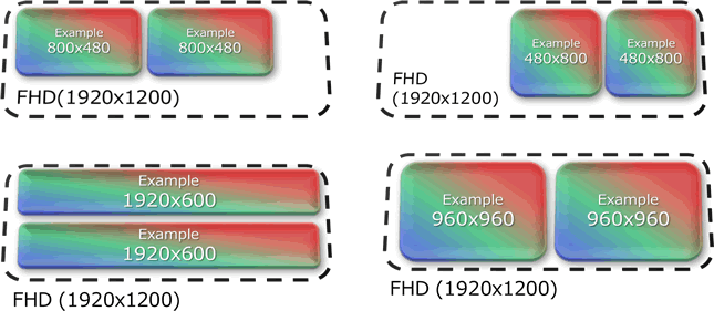
Splitter Function(Line or LR split)
Resolution size : Possible to sprit dual display within 1920×1080 resolution.
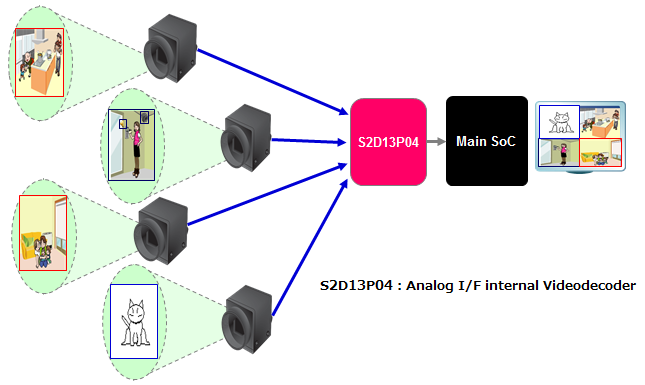
 Epson camera interface ICs is suitable for the multi camera system. They have the camera inputs of 4 channels and output with 4 kinds of modes; fixed chanel, mergence, auto scan, and compression. Because VRAM for the picture processing is built into, the camera interface of 4into1 can be achieved by single-chip.The number of the camera can be easily increased without any change from 1 camera system.
| Status | Download | Model name | Outline |
|---|---|---|---|
| MP | Document download | S2D13P04 | The S2D13P04 supports the NTSC/PAL signal. 4 video decoders are implemented to each 4 channels input independently,and video signal isoutput by stable frame rate. |
| MP | S2S65P10 | The S2S65P10 converts the interlace signal into the progressive signal. The digital output of the NTSC/PAL video decoder can be converted into progressive. |